

Programmable Logic?

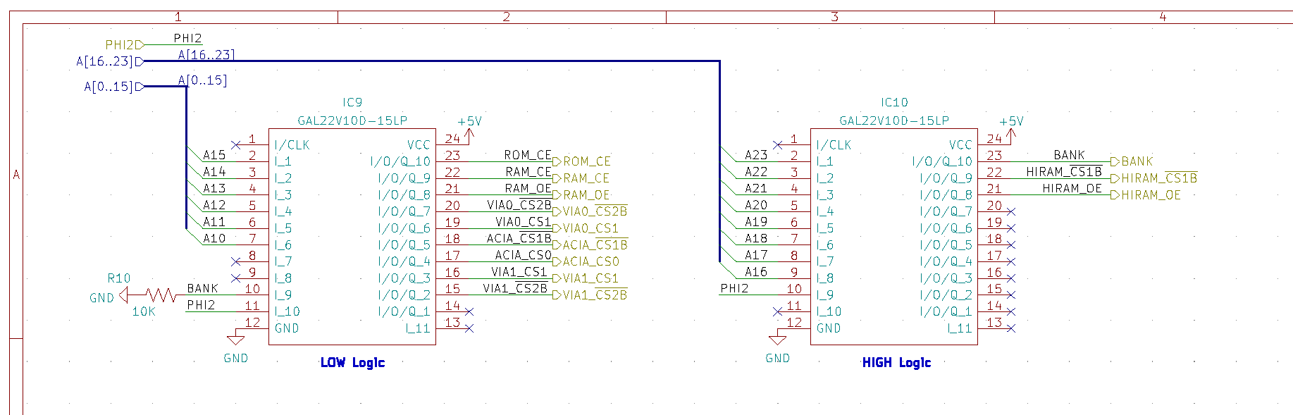
Two ATF22V10C-7PX Chips for High and Low address logic.
So initially I wanted to do everything in discreet logic. But honestly, that’s a pain in the ass. And for the 6502 phase of the project I did use discreet logic. But that was a simpler project in a simpler time. My first thoughts on using programmable logic were pretty negative. But someone on /r/beneater put it best. Commodore had a whole chip fab to make custom chips, and we don’t. And they made the PLA, CIA, VIC, SID, etc. Also, GALs existed at the time so I’m one hundred percent ok with this decision now.
Writing the logic
So I have never written programmable logic before. But I have seen people use the program Digital to design it. Turns out that can output to JEDEC files! So no having to deal with the archaic WinCUPL.
And the default programmer for the TL-866II+ can read and write JEDEC files! 🥳
The initial writes seemed to work just fine. They wrote in and ready back properly. Now I just need to see if they work in the board! Luckily the NS65816 was designed around these chips and the pinout I wrote for the logic, go figure!
Keeping it organized
My label maker can print small enough but I had to cut down the labels to put on the top.
Since I designed the logic to be two matching chips, it would be easy to get them confused. And they’re skinny DIPs, so a big label just doesn’t fit. It’s annoying, but I can work with it. I think I could get the Hi-RAM into a 16V8 for now, but I want to leave the space for expansion as the board grows.
I like the 22V10 chips for the fact that pins 14 through 23 can be input or output, in case I need more inputs.
Logic Chip Current Layout as of April 2022
The low logic is pretty well set, as it’s designed to mimic the design of my 6502 computer for now. The up side is that if I decide to relocate things in the low memory space, it’s completely possible. As you can see it’s controlling two VIAs and the 6551 (ACIA). Between that and the system ROM and Low-RAM, it’s a pretty full 64K.
The current Bank $00 (<64K) map looks like this:
$0000 - $3FFF (16K) System/Low RAM
$4000 - $7FFF (16K) Reserved for Peripherals
$6000 - $600F - VIA 0 - LCD and RTC
$6010 - $601F - VIA 1 - Diagnostic Lights
$6800 - $6804 - ACIA (WDC65C51) for Serial communications
$8000 - $FFFF (32K) Kernel ROM
The plan is to add a VIA, PIA, or some other controller chip for the PS/2 interface for the keyboard, and whatever it takes to run 4 SNES controllers.
At the moment I’m not planning on adding a mouse, but that’s not to say it can’t be part of the design later.